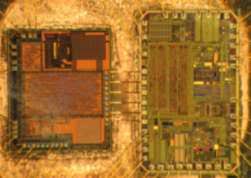
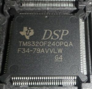
Break texas instrument microcontroller tms320f240pqa’s security fuse bit by focus ion beam to reset its status, then will have chance to execute TI DSP Controller TMS320F240PQA Code Extraction, the embedded firmware can be cloned directly from TMS320F240PQA flash memory;

The functional block diagram provides a high-level description of each component in the F243/F241 DSP controllers which has become quite common in copying ti tms320f28030 dsp mcu flash program. The TMS320x24x devices are composed of three main functional units: a C2xx DSP core, internal memory, and peripherals. In addition to these three functional units, there are several system-level features of the F243/F241 that are distributed.
These system features include the memory map, device reset, interrupts, digital input / output (I / O), clock generation, and low-power operation.

‡ When CNF = 0, addresses 0100h−01FFh and 0200h−02FFh are mapped to the same physical block (B0) in data-memory space. For example,
a write to 0100h will have the same effect as a write to 0200h. For simplicity, addresses 0100h−01FFh are referred to as reserved.
§ Addresses 0300h−03FFh and 0400h−04FFh are mapped to the same physical block (B1) in data-memory space. For example, a write to 0400h has the same effect as a write to 0300h. For simplicity, addresses 0400h−04FFh are referred to as Reserved.
The F243/F241 devices implement three separate address spaces for program memory, data memory, and I/O space. On the F243/F241, the first 96 (0−5Fh) data memory locations are either allocated for memory-mapped registers or reserved which can be used for tms320f28035 microprocessor flash memory copying. This memory-mapped register space contains various control and status registers, including those for the CPU. All the on-chip peripherals of the F243/F241 devices are mapped into data memory space. Access to these registers is made by the CPU instructions addressing their data memory locations. Figure 1 shows the F243 memory map and Figure 2 shows the F241 memory map.

