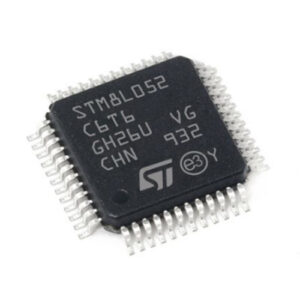
STM8L052C6T6 IC MCU Flash Code Extraction is a process to unlock the protection mechanism against stm8l052c6 microcontroller flash memory, and then decrypt copied firmware from heximal to asm language;

The high-density and medium+ density STM8L15xx6/8x devices feature a nested vectored interrupt controller:
Nested interrupts with 3 software priority levels
32 interrupt vectors with hardware priority
Up to 40 external interrupt sources on 11 vectors
The device requires a 1.65 V to 3.6 V operating supply voltage (VDD). The external power supply pins must be connected as follows in the process of clone stm32f107vct mcu flash memory data:
VSS1, VDD1, VSS2, VDD2, VSS3, VDD3, VSS4, VDD4= 1.65 to 3.6 V: external power supply for I/Os and for the internal regulator. Provided externally through VDD pins, the corresponding ground pin is VSS. VSS1/VSS2/VSS3/VSS4 and VDD1/VDD2/VDD3/VDD4 must not be left unconnected.

VSSA, VDDA = 1.65 to 3.6 V: external power supplies for analog peripherals (minimum voltage to be applied to VDDA is 1.8 V when the ADC1 is used). VDDA and VSSA must be connected to VDD and VSS, respectively.
VREF+, VREF- (for ADC1): external reference voltage for ADC1. Must be provided externally through VREF+ and VREF- pin.
VREF+ (for DAC1/2): external voltage reference for DAC1 and DAC2 must be provided externally through VREF+.

