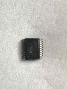
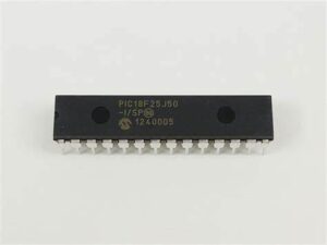
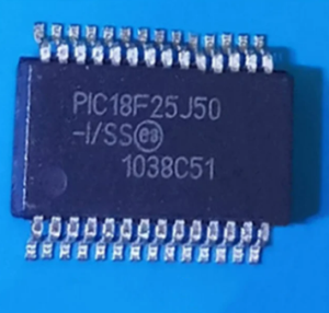
Read PIC18F25J50 Microprocessor Flash Program out from its flash and eeprom memory, the program format will be in binary or heximal, fuse bit of microcontroller pic18f25k50 will be cracked, and then restore memory file from pic18f25j50 MCU;

Data is received at the RX/DT pin. The RX/DT pin output driver is automatically disabled when the EUSART is configured for synchronous master receive operation by Read PIC18F25J50 Microprocessor Flash Program. In Synchronous mode, reception is enabled by setting either the Single Receive Enable bit (SREN of the RCSTA register) or the Continuous Receive Enable bit (CREN of the RCSTA register) after Read Microcontroller ATTINY12 Firmware.

When SREN is set and CREN is clear, only as many clock cycles are generated as there are data bits in a single character. The SREN bit is automatically cleared at the completion of one character before Read IC ATTINY11 Software. When CREN is set, clocks are continuously generated until CREN is cleared.
If CREN is cleared in the middle of a character the CK clock stops immediately and the partial character is discarded. If SREN and CREN are both set, then SREN is cleared at the completion of the first character and CREN takes precedence for the purpose of Extract IC AT90S2313 Firmware.

To initiate reception, set either SREN or CREN. Data is sampled at the RX/DT pin on the trailing edge of the TX/CK clock pin and is shifted into the Receive Shift Register (RSR) in order to Extract MCU AT90S1200 Code.
When a complete character is received into the RSR, the RCIF bit is set and the character is automatically transferred to the two character receive FIFO. The Least Significant eight bits of the top character in the receive FIFO are available in RCREG before Crack MCU Flash. The RCIF bit remains set as long as there are unread characters in the receive FIFO.


