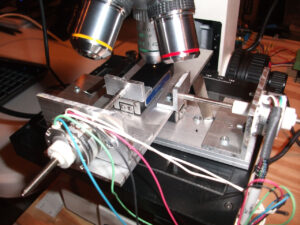
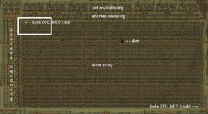
The PIC18F8493 microprocessor is a powerful MCU, often used in embedded systems. However, accessing its internal memory to extract or modify data can present a challenge, especially when the memory is protected or encrypted. To read the microprocessor’s internal memory, one needs to use reverse engineering techniques, which may include cracking or hacking into the device to bypass security measures.

First, it’s important to understand that the firmware or binary data stored in the microcontroller PIC18F8493’s EEPROM or flash memory can be locked or encrypted for protection. In such cases, one must employ methods like decapsulating the chip to physically access the microcontroller, or use a debugger to crack the protection.

Once access is gained, the data can be extracted, decrypted, or decoded. Reverse engineering may be necessary to recover the source code or dump the entire memory contents into a file for further analysis. If the firmware is secured, techniques like cloning or replicating the chip can be used to create a duplicate microprocessor, allowing further exploration without risking damage to the original chip.

The process requires careful attention to detail, as improper handling can result in corrupted data or permanent damage to the microcontroller.
We can Read Microprocessor PIC18F8493 Internal Memory, please view the Microprocessor PIC18F8493 features for your reference:
External interrupts on the RA0/INT0, RA1/INT1, RB2/INT2 and RB3/INT3 pins are edge-triggered. If the corresponding INTEDGx bit in the INTCON2 register is set (= 1), the interrupt is triggered by a rising edge; if the bit is clear, the trigger is on the falling edge to faciliate the process of Extract Microchip MCU PIC16F917 Code. When a valid edge appears on the pin, the corresponding flag bit, INTxIF, is set.
This interrupt can be disabled by clearing the corresponding enable bit, INTxIE. Flag bit, INTxIF, must be cleared in software in the Interrupt Service Routine before re-enabling the interrupt for MCU Crack. All external interrupts (INT0, INT1, INT2 and INT3) can wake-up the processor from Idle or Sleep modes if bit INTxIE was set prior to going into those modes when Read Microprocessor PIC18F8493 Internal Memory.
If the Global Interrupt Enable bit, GIE, is set, the processor will branch to the interrupt vector following wake-up. Interrupt priority for INT1, INT2 and INT3 is determined by the value contained in the interrupt priority bits, INT1IP (INTCON3<6>), INT2IP (INTCON3<7>) and INT3IP (INTCON2<1>). There is no priority bit associated with INT0. It is always a high priority interrupt source only after Reading Locked PIC16F916 Flash.
In 8-bit mode (which is the default), an overflow in the TMR0 register (FFh → 00h) will set flag bit, TMR0IF. In 16-bit mode, an overflow in the TMR0H:TMR0L register pair (FFFFh → 0000h) will set TMR0IF. The interrupt can be enabled/disabled by setting/clearing enable bit, TMR0IE (INTCON<5>) after Read Microprocessor PIC18F8493 Internal Memory.
Interrupt priority for Timer0 is determined by the value contained in the interrupt priority bit, TMR0IP (INTCON2<2>). See Section 11.0 “Timer0 Module” for further details on the Timer0 module. An input change on PORTA<1:0> and/or PORTB<2:3> sets flag bit, RBIF (INTCON<0>) to in the process of Read Out Microcontroller PIC16F690 Program. The interrupt can be enabled/disabled by setting/clearing enable bit, RBIE (INTCON<3>). Interrupt priority for interrupt-on-change is determined by the value contained in the interrupt priority bit, RBIP (INTCON2<0>).

