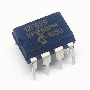
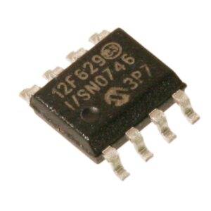
Read MCU PIC12F629 Archive from microcontroller PIC12F629 program memory and data eeprom, this process can help to recover firmware from Microprocessor memory through MCU crack method;

Each PORTA pin is multiplexed with other functions. The pins and their combined functions are briefly described here. For specific information about individual functions such as the comparator or the A/D Converter (ADC), refer to the appropriate section in this data sheet.
Figure 4-2 shows the diagram for this pin. The RA0/AN0/C1IN+/ICSPDAT/ULPWU pin is configurable to function as one of the following:
a general purpose I/O which can be used for semi-invasive IC mcu code extraction
an analog input for the ADC (except PIC16F631)
an analog input to Comparator C1
In-Circuit Serial Programming™ data
an analog input for the Ultra Low-Power Wake-up
Figure 4-2 shows the diagram for this pin. The RA1/AN1/C12IN0-/VREF/ICSPCLK pin is configurable to function as one of the following:
a general purpose I/O
an analog input for the ADC (except PIC16F631)
an analog input to Comparator C1 or C2
a voltage reference input for the ADC
In-Circuit Serial Programming clock
Figure 4-3 shows the diagram for this pin. The
RA2/AN2/T0CKI/INT/C1OUT pin is configurable to function as one of the following:
a general purpose I/O able to help remove microcontroller protection for copying
an analog input for the ADC (except PIC16F631)
the clock input for TMR0
an external edge triggered interrupt
a digital output from Comparator C1

Figure 4-4 shows the diagram for this pin. The RA3/MCLR/VPP pin is configurable to function as one of the following:
- a general purpose input
- as Master Clear Reset with weak pull-upFigure 4-5 shows the diagram for this pin. The
RA4/AN3/T1G/OSC2/CLKOUT pin is configurable to function as one of the following:
a general purpose I/Oan analog input for the ADC (except PIC16F631)
a TMR1 gate input
a crystal/resonator connectiona clock output
PORTB is a 4-bit wide, bidirectional port. The corresponding data direction register is TRISB (Register 4-6). Setting a TRISB bit (= 1) will make the corresponding PORTB pin an input (i.e., put the corresponding output driver in a High-Impedance mode).
Clearing a TRISB bit (= 0) will make the corresponding PORTB pin an output (i.e., enable the output driver and put the contents of the output latch on the selected pin). Example 4-3 shows how to initialize PORTB. Reading the PORTB register (Register 4-5) reads the status of the pins, whereas writing to it will write to the PORT latch.
- All write operations are read-modify-write operations. Therefore, a write to a port implies that the port pins are read, this value is modified and then written to the PORT data latch.

