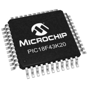
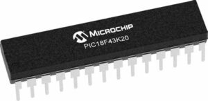
MCU PIC18F43K20 Secured Memory Program Replication has to firstly break Microcontroller pic18f43k20 silicon package with decapsulation technique and crack mcu pic18f43k20 fuse bit which embedded inside the memory;

The use of Indexed Literal Offset Addressing mode effectively changes how the first 96 locations of Access RAM (00h to 5Fh) are mapped. Rather than containing just the contents of the bottom section of Bank 0, this mode maps the contents from a user defined “window” that can be located anywhere in the data memory space which can help to extract mcu pic18f13k50 flash memory.
The value of FSR2 establishes the lower bound- ary of the addresses mapped into the window, while the upper boundary is defined by FSR2 plus 95 (5Fh). Addresses in the Access RAM above 5Fh are mapped as previously described, An example of Access Bank remapping in this addressing mode.

Remapping of the Access Bank applies only to operations using the Indexed Literal Offset mode. Operations that use the BSR (Access RAM bit is ‘1’) will continue to use direct addressing as before.
Enabling the extended instruction set adds eight additional commands to the existing PIC18 instruction set. These instructions are executed as described in Section 24.2 “Extended Instruction Set”


