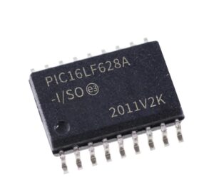
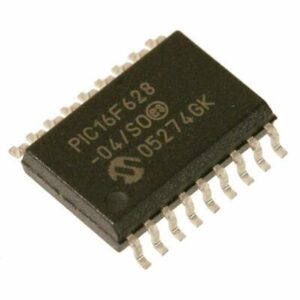
Extract MCU PIC16LF628A Code needs to unlock microcontroller pic16lf628a flash by focus ion beam, and then recover MCU heximal from open master MCU;

This section is not applicable to the PIC16LF628A. PORTE has three pins, RE0/RD/AN5, RE1/WR/AN6 and RE2/CS/AN7, which are individually configureable as inputs or outputs.
These pins have Schmitt Trigger input buffer. I/O PORTE becomes control inputs for the microprocessor port when bit PSPMODE (TRISE<4>) is set if copy atmega1281pv MCU bin.
In this mode, the user must make sure that the TRISE<2:0> bits are set (pins are configured as digital inputs). Ensure ADCON1 is configured for digital I/O. In this mode, the input buffers are TTL.
Register 4-1 shows the TRISE register, which also controls the parallel slave port operation. PORTE pins are multiplexed with analog inputs. When selected as an analog input, these pins will read as ’0’s.
TRISE controls the direction of the RE pins, even when they are being used as analog inputs. The user must make sure to keep the pins configured as inputs when using them as analog inputs when copy atmega1281pa MCU code.
The Parallel Slave Port (PSP) is not implemented on the PIC16LF628A. PORTD operates as an 8-bit wide Parallel Slave Port, or Microprocessor Port, when control bit PSPMODE (TRISE<4>) is set.

In Slave mode, it is asynchronously readable and writable by an external system using the read control input pin RE0/RD, the write control input pin RE1/WR, and the chip select control input pin RE2/CS.
The PSP can directly interface to an 8-bit microprocessor data bus. The external microprocessor can read or write the PORTD latch as an 8-bit latch. Setting bit PSPMODE enables port pin RE0/RD to be the RD input, RE1/WR to be the WR input and RE2/CS to be the CS (chip select) input after Extract copy atmega2560a MCU hex code.
For this functionality, the corresponding data direction bits of the TRISE register (TRISE<2:0>) must be configured as inputs (i.e., set). The A/D port configuration bits PCFG3:PCFG0 RE2:RE0 as digital I/O.

