Extract MCU AT89C51AC3 Code out from flash and eeprom memory after unlock microcontroller, the status of MCU will be reset from encrypted to decrypted by cut off the security fuse bit;
How to Extract MCU AT89C51AC3 Code: Overcoming Secured Firmware Barriers
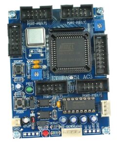
The task to extract MCU AT89C51AC3 code is one of the most technically demanding processes in the field of embedded security. The AT89C51AC3, a powerful microcontroller from Atmel (now part of Microchip), features advanced capabilities including an integrated 16-bit timer, enhanced UART, and a high-performance flash memory system. These features make the chip ideal for industrial and automotive applications, but they also pose significant challenges when attempting to access its locked or encrypted firmware.
Unique Features of AT89C51AC3
The AT89C51AC3 microcontroller is built on the 8051 architecture and offers a high-speed flash memory (up to 64KB) and 2KB of EEPROM, with support for ISP (In-System Programming) and IAP (In-Application Programming). It also incorporates hardware-level encryption and locking mechanisms that protect the flash memory against unauthorized access.
These protected features make it extremely difficult to extract, copy, or replicate the firmware. The secured program memory and data archives within the chip are resistant to traditional code recovery methods. As a result, any attempt to dump or decode the binary must overcome robust security protocols.
Techniques to Extract AT89C51AC3 Code
-
Decapsulation and Microprobing: This physical attack involves opening the chip package to expose the silicon die. Engineers can then use microscopic probes to read the contents of the flash memory, bypassing the encrypted and locked memory areas.
-
Fault Injection Attacks: Voltage or clock glitching techniques may allow attackers to break the microcontroller’s protection momentarily, enabling partial firmware dumping or memory access.
-
Firmware Cloning and Replication: Forensic analysis and reverse engineering tools may be used to replicate the MCU behavior by analyzing any available binary or partially recovered source code.
-
Custom Interface Exploits: Some devices using the AT89C51AC3 chip may have unsecured debugging interfaces. Skilled researchers can exploit these interfaces to gain access to memory and program files.
Professional Code Extraction Services
Given the complexity of this process, professional services specializing in MCU code extraction offer tailored solutions. Our lab provides a unique service to extract firmware from AT89C51AC3 microcontrollers, using a combination of hardware attacks and software decryption techniques. With years of experience in secured firmware recovery, we can help clients decrypt, dump, and duplicate program data for legitimate and authorized purposes.
We ensure full confidentiality and legal compliance, working only with customers who have rightful ownership or authorization to access the protected firmware. Whether you need to recover lost source code, decode encrypted memory contents, or clone a microcontroller for legacy system replication, we offer an end-to-end solution.
Conclusion
Extracting the AT89C51AC3 MCU code is a specialized task requiring advanced knowledge and tools. The secured flash memory, encrypted EEPROM, and locked program files make it extremely difficult to recover the firmware without expert intervention. Our code extraction services provide a reliable and legally compliant pathway to replicate, recover, or decode protected data from this robust microcontroller chip.
फ़र्मवेयर क्लोनिंग और प्रतिकृति: किसी भी उपलब्ध बाइनरी या आंशिक रूप से पुनर्प्राप्त स्रोत कोड का विश्लेषण करके MCU व्यवहार को दोहराने के लिए फोरेंसिक विश्लेषण और रिवर्स इंजीनियरिंग टूल का उपयोग किया जा सकता है।, कस्टम इंटरफ़ेस एक्सप्लॉइट्स: AT89C51AC3 चिप का उपयोग करने वाले कुछ डिवाइस में असुरक्षित डिबगिंग इंटरफ़ेस हो सकते हैं। कुशल शोधकर्ता मेमोरी और प्रोग्राम फ़ाइलों तक पहुँच प्राप्त करने के लिए इन इंटरफ़ेस का उपयोग कर सकते हैं।
Software can take advantage of the additional data pointers to both increase speed and reduce code size, for example, block operations (copy, compare…) are well served by using one data pointer as a “source” pointer and the other one as a “destination” pointer.
Hereafter is an example of block move implementation using the two pointers and coded in assembler. The latest C compiler takes also advantage of this feature by providing enhanced algorithm libraries. The INC instruction is a short (2 Bytes) and fast (6 machine cycle) way to manipulate the DPS bit in the AUXR1 register. However, note that the INC instruction does not directly force the DPS bit to a particular state, but simply toggles it. In simple routines, such as the block move example, only the fact that DPS is toggled in the proper sequence matters, not its actual value. In other words, the block move routine works the same whether DPS is ‘0’ or ‘1’ on entry.
Note:
If VCC was reduced during the Power-Down mode, do not exit Power-Down mode until VCC is restored to the normal operating level. There are two ways to exit the Power-Down mode:
- Generate an enabled external interrupt.
Note:
The AT89C51AC3 provides capability to exit from Power-Down using INT0#, INT1#. Hardware clears PD bit in PCON register which starts the oscillator and restores the clocks to the CPU and peripherals. Using INTx# input, execution resumes when the input is released (see Figure 19). Execution resumes with the interrupt service routine. Upon completion of the interrupt service routine, program execution resumes with the instruction immediately following the instruction that activated Power-Down mode before Extract microcontroller embedded firmware.
The external interrupt used to exit Power-Down mode must be configured as level sensitive (INT0# and INT1#) and must be assigned the highest priority. In addition, the duration of the interrupt must be long enough to allow the oscillator to stabilize. The execution will only resume when the interrupt is deasserted. Exit from power-down by external interrupt does not affect the SFRs nor the internal RAM content.
The 2-Kbyte on-chip EEPROM memory block is located at addresses 0000h to 07FFh of the XRAM/ERAM memory space and is selected by setting control bits in the EECON register. A read in the EEPROM memory is done with a MOVX instruction. A physical write in the EEPROM memory is done in two steps: write data in the column latches and transfer of all data latches into an EEPROM memory row (programming).
The number of data written on the page may vary from 1 up to 128 Bytes (the page size). When programming, only the data written in the column latch is programmed and a ninth bit is used to obtain this feature. This provides the capability to program the whole memory by Bytes, by page or by a number of Bytes in a page. Indeed, each ninth bit is set when the writing the corresponding byte in a row and all these ninth bits are reset after the writing of the complete EEPROM row.
The EEPROM programming consists of the following actions:
writing one or more Bytes of one page in the column latches. Normally, all Bytes must belong to the same page; if not, the first page address will be latched and the others discarded.
launching programming by writing the control sequence (50h followed by A0h) to the EECON register. EEBUSY flag in EECON is then set by hardware to indicate that programming is in progress and that the EEPROM segment is not available for reading. The end of programming is indicated by a hardware clear of the EEBUSY flag.