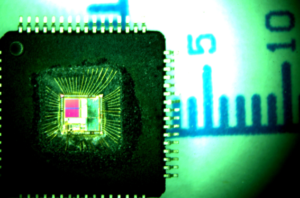
The first step to Extract DSP Microcontroller TMS320F28022 Source Code is to reverse engineering dsp mcu tms320f28022 and locate its security fuse bit, unlock the dsp processor tms320f28022 tamper resistance system;

As with many DSP type devices, multiple busses are used to move data between the memories and peripherals and the CPU. The C28x memory bus architecture contains a program read bus, data read bus and data write bus. The program read bus consists of 22 address lines and 32 data lines.

The data read and write busses consist of 32 address lines and 32 data lines each. The 32-bit-wide data busses enable single cycle 32-bit operations. The multiple bus architecture, commonly termed Harvard Bus, enables the C28x to fetch an instruction, read a data value and write a data value in a single cycle.
All peripherals and memories attached to the memory bus will prioritize memory accesses to readout dsp mcu tms320f28015 flash binary file. Generally, the priority of memory bus accesses can be summarized as follows:
Highest:
Data Writes (Simultaneous data and program writes cannot occur on the memory bus.)
Program Writes (Simultaneous data and program writes cannot occur on the memory bus.)
Data Reads Program (Simultaneous program reads and fetches cannot occur on the Reads memory bus.) is a functions to extract mcu tms320f28016 firmware file from its embedded memory
Lowest:
Fetches (Simultaneous program reads and fetches cannot occur on the memory bus.)

