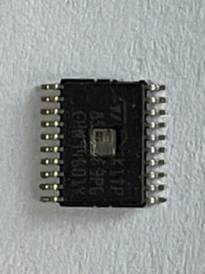
Extract Code of Microcontroller PIC18F8393 needs to crack microprocessor pic18f8393 protective fuse bit, restoring ic chip embedded information from it;

The SPI mode allows 8 bits of data to be synchronously transmitted and received simultaneously. All four modes of SPI are supported. To accomplish communication, typically three pins are used:• Serial Data Out (SDO) – RC5/SDO
• Serial Data In (SDI) – RC4/SDI/SDA
• Serial Clock (SCK) – RC3/SCK/SCL
Additionally, a fourth pin may be used when in a Slave mode of operation:
• Slave Select (SS) – RA5/SS
Figure 17-1 shows the block diagram of the MSSP module when operating in SPI mode.
The MSSP module has four registers for SPI mode operation when extract firmware of MCU. These are:
- MSSP Control Register 1 (SSPCON1)
- MSSP Status Register (SSPSTAT)
- Serial Receive/Transmit Buffer Register (SSPBUF)
- MSSP Shift Register (SSPSR) – Not directly accessible
SSPCON1 and SSPSTAT are the control and status registers in SPI mode operation. The SSPCON1 register is readable and writable. The lower 6 bits of the SSPSTAT are read-only. The upper two bits of the SSPSTAT are read/write. SSPSR is the shift register used for shifting data in or out. SSPBUF is the buffer register to which data bytes are written to or read from or content of IC extraction.
In receive operations, SSPSR and SSPBUF together create a double-buffered receiver. When SSPSR receives a complete byte, it is transferred to SSPBUF and the SSPIF interrupt is set. During transmission, the SSPBUF is not double buffered. A write to SSPBUF will write to both SSPBUF and SSPSR.
When initializing the SPI, several options need to be specified. This is done by programming the appropriate control bits (SSPCON1<5:0> and SSPSTAT<7:6>).
These control bits allow the following to be specified:••••• Master mode (SCK is the clock output)Slave mode (SCK is the clock input)Clock Polarity (Idle state of SCK)Data Input Sample Phase (middle or end of data output time)
- Clock Edge (output data on rising/falling edge of SCK)
- Clock Rate (Master mode only) after the Microcontroller binary extraction
- Slave Select mode (Slave mode only)
The MSSP consists of a transmit/receive shift register (SSPSR) and a buffer register (SSPBUF). The SSPSR shifts the data in and out of the device, MSb first. The SSPBUF holds the data that was written to the SSPSR until the received data is ready. Once the 8 bits of data have been received, that byte is moved to the SSPBUF register. Then, the Buffer Full detect bit, BF (SSPSTAT<0>) and the interrupt flag bit, SSPIF, are set. This double-buffering of the received data (SSPBUF) allows the next byte to start reception before Unlocking MCU data that was just received.
Any write to the SSPBUF register during transmission/reception of data will be ignored and the write collision detect bit, WCOL (SSPCON1<7>), will be set. User software must clear the WCOL bit so that it can be determined if the following write(s) to the SSPBUF register completed successfully.

