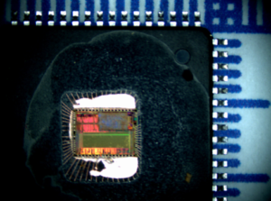
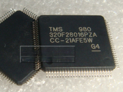
DSP TMS320F28016 MCU Firmware Extraction will need to reverse engineering tms320f28016 microcontroller system and then unlock tms320f28016 protective mechanism by breaking off its fuse bit;

Interface to memory and I/O devices of varying speeds is accomplished by using the READY input. When transactions are made with slower devices, the TMS320F28016 processor waits until the other device completes its function and signals the processor by way of the READY input from Unlock TMS320F28016 DSP Microcontroller Memory Heximal.

Once a ready indication is provided from the external device, execution continues. On the ’x240 device, the READY input must be driven (active high) to complete reads or writes to internal data I/O-memory-mapped registers and all external addresses only to restore dsp mcu embedded firmware from tms320f28232 mcu.
The bus request (BR) signal is used in conjunction with the other TMS320F28016 interface signals to arbitrate external global-memory accesses. Global memory is external data-memory space in which the BR signal is asserted at the beginning of the access. When an external global-memory device receives the bus request, it responds by asserting the ready signal after the global-memory access is arbitrated and the global access is completed.
The TMS320F28016 supports zero-wait-state reads on the external interface. However, to avoid bus conflicts, writes take two cycles. This allows the ’x240 to buffer the transition of the data bus from input to output (or output to input) by a half cycle. In most systems, TMS320F28016 ratio of reads to writes is significantly large to minimize the overhead of the extra cycle on writes.
Wait states can be generated when accessing slower external resources. The wait states operate on machine-cycle boundaries and are initiated either by using the ready signal or using the software wait-state generator to readout microprocessor tms320f28016 flash binary. Ready can be used to generate any number of wait states.

