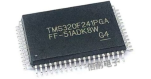
DSP Microcontroller TMS320F241PGA Flash Program Duplication can help engineer to restore embedded binary file from dsp chip tms320f241pga memory after attack mcu tms320f241pga security system;

Device reset. RS causes the F243/241 to terminate execution and sets PC = 0. When RS is brought to a high level, execution begins at location zero of program memory. RS affects (or sets to zero) various registers and status bits. When the watchdog timer overflows, it initiates a system reset pulse that is reflected on the RS pin. This pulse is eight clock cycles wide.
Nonmaskable interrupt. When NMI is activated, the device is interrupted regardless of the state of the INTM bit of the status register. NMI is (falling) edge- and low-level-sensitive in the process of readout dsp controller tms320f240pgs flash binary. To be recognized by the core, this pin must be kept low for at least one clock cycle after the falling edge.
External user interrupt 1 or GPIO. Both XINT1 and XINT2 are edge- sensitive. To be recognized by the core, these pins must be kept high/low for at least one clock cycle after the edge. The edge polarity is programmable.
External user interrupt 2. External “start-of-conversion” input for ADC/GPIO. Both XINT1 and XINT2 are edge-sensitive. To be recognized by the core, these pins must be kept high/low for at least one clock cycle after the edge. The edge polarity is programmable which is easier for extract dsp controller tms320f240pga code file.

