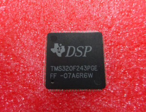
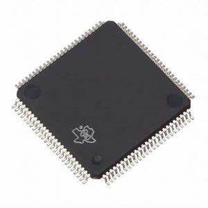
Readout DSP Chip TMS320F243PGE Flash Data and copy the heximal file to new microcontroller tms320f243pge, original mcu ic tms320f243pge will be cracked and locked bit which has been used to protect the readout execution on the microprocessor has been disabled by invasive attack;

The control structure for shared I/O pins is shown in Figure 4, where each pin has three bits that define its operation:
- Mux control bit — this bit selects between the primary function (1) and I/O function (0) of the pin.
- I/O direction bit — if the I/O function is selected for the pin (mux control bit is set to 0), this bit determines whether the pin is an input (0) or an output (1).
- I/O data bit — if the I/O function is selected for the pin (mux control bit is set to 0) and the direction selected is an input, data is read from this bit; if the direction selected is an output, data is written to this bit.
The mux control bit, I/O direction bit, and I/O data bit are in the I/O control registers.

The TMS320x24x software-programmable interrupt structure supports flexible on-chip and external interrupt configurations to meet real-time interrupt-driven application requirements. The F243/F241 recognizes three types of interrupt sources:
- Reset (hardware- or software-initiated) is unarbitrated by the CPU and takes immediate priority over any other executing functions. All maskable interrupts are disabled until the reset service routine enables them.
The F243/F241 devices have two sources of reset: an external reset pin and a watchdog timer timeout (reset).

