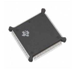
Readout DSP Processor TMS320F240PQS Flash Binary needs to break the protection over mcu chip tms320f240pqs flash memory, and then clone program to new dsp microcontroller tms320f240pqs;

Due to the fast cycle time of the F243 devices, it is often necessary to operate with wait states to interface with external logic or memory. For many systems, one wait state is adequate. The software wait-state generator can be programmed to generate between 0 and 7 wait states for a given space.
Software wait states are configured through the wait-state generator register (WSGR). The WSGR includes three 3-bit fields to configure wait states for the following external memory spaces: data space (DSWS), program space (PSWS), and I/O space (ISWS) in the process of dsp microcontroller tms320f28023 flash program extraction. The wait-state generator enables wait states for a given memory space based on the value of the corresponding three bits, regardless of the condition of the READY signal.


The READY signal can be used to generate additional wait states. All bits of the WSGR are set to 1 at reset so that the device can operate from slow memory at reset in order to copy microcontroller tms320f28026 flash memory program. The WSGR register (shown in Table 3, Table 4 and Table 5) resides at I / O location FFFFh. This register should not be accessed in the F241

