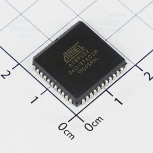
Extract MCU AT89S52 Binary from its memory, the firmware can be copied to blank Microcontroller AT89S52 which will provide the same functions as original version, disable the security fuse bit by focus ion beam technique, which is critical step for MCU Cracking;
If you need to extract the MCU AT89S52 binary from a secured or locked chip, our professional services can assist you in breaking through various protection mechanisms. Whether your microcontroller is encrypted, locked, or protected, we specialize in recovering, copying, and duplicating firmware, program memory, and EEPROM data.
Advanced Techniques to Unlock Secured AT89S52 Chips
The AT89S52 microcontroller is a widely used 8-bit chip with flash memory that is often secured to prevent unauthorized access. However, for legitimate purposes such as system recovery, reverse engineering, or replication, we employ advanced techniques to:
-
Dump and Decode Firmware – We can retrieve and decrypt locked binary files from the chip.
-
Copy and Clone Protected Data – Our methods ensure the replication of essential microcontroller data.
-
Recover and Extract EEPROM/Flash – We specialize in accessing secured flash memory and EEPROM archives.
-
Break Encryption and Decrypt Source Code – When necessary, we use innovative attack strategies to bypass encryption.
-
Decapsulate and Analyze Chip Structures – For more complex protection schemes, we can physically analyze and recover the microprocessor’s content.
Professional MCU Binary Extraction Services
With years of experience in microcontroller security analysis, we offer a reliable and efficient way to extract, recover, and duplicate the AT89S52 firmware, even from highly secured environments. If you need to access protected MCU files, restore lost program memory, or replicate an existing system, our expert team is here to help.
Contact us today for professional assistance in unlocking your secured microcontroller and recovering essential firmware and data!
Port 0 is an 8-bit open drain bidirectional I/O port. As an output port, each pin can sink eight TTL inputs. When 1s are written to port 0 pins, the pins can be used as high-impedance inputs. Port 0 can also be configured to be the multiplexed low-order address/data bus during accesses to external program and data memory. In this mode, P0 has internal pullups.
Port 0 also receives the code bytes during Flash programming and outputs the code bytes during program verification. External pullups are required during program verification. Port 1 is an 8-bit bidirectional I/O port with internal pullups. The Port 1 output buffers can sink/source four TTL inputs if Extract Microcontroller at89c55 code.
अपने सुरक्षित माइक्रोकंट्रोलर को अनलॉक करने और आवश्यक फ़र्मवेयर और डेटा को पुनर्प्राप्त करने में पेशेवर सहायता के लिए आज ही हमसे संपर्क करें!
When 1s are written to Port 1 pins, they are pulled high by the internal pullups and can be used as inputs. As inputs, Port 1 pins that are externally being pulled low will source current (IIL) because of the internal pullups. In addition, P1.0 and P1.1 can be configured to be the timer/counter 2 external count input (P1.0/T2) and the timer/counter 2 trigger input (P1.1/T2EX), respectively, as shown in the following table.
Port 1 also receives the low-order address bytes during Flash programming and verification. Port 2 is an 8-bit bidirectional I/O port with internal pullups. The Port 2 output buffers can sink/source four TTL inputs. When 1s are written to Port 2 pins, they are pulled high by the internal pullups and can be used as inputs. As inputs, Port 2 pins that are externally being pulled low will source current (IIL) because of the internal pullups.
Port 2 emits the high-order address byte during fetches from external program memory and during accesses to external data memory that use 16-bit addresses (MOVX @ DPTR). In this application, Port 2 uses strong internal pullups when emitting 1s. During accesses to external data memory that use 8-bit addresses (MOVX @ RI), Port 2 emits the contents of the P2 Special Function Register if Extract chip firmware.
Port 2 also receives the high-order address bits and some control signals during Flash programming and verification. Port 3 is an 8-bit bidirectional I/O port with internal pullups. The Port 3 output buffers can sink/source four TTL inputs. When 1s are written to Port 3 pins, they are pulled high by the internal pullups and can be used as inputs. As inputs, Port 3 pins that are externally being pulled low will source current (IIL) because of the pullups.
Port 3 also serves the functions of various special features of the AT89S52, as shown in the following table. Port 3 also receives some control signals for Flash programming and verification.
Reset input. A high on this pin for two machine cycles while the oscillator is running resets the device. This pin drives High for 96 oscillator periods after the Watchdog times out. The DISRTO bit in SFR AUXR (address 8EH) can be used to disable this feature. In the default state of bit DISRTO, the RESET HIGH out feature is enabled after Extract chip binary.
Address Latch Enable (ALE) is an output pulse for latching the low byte of the address during accesses to external memory. This pin is also the program pulse input (PROG) during Flash programming. In normal operation, ALE is emitted at a constant rate of 1/6 the oscillator frequency and may be used for external timing or clocking purposes. Note, however, that one ALE pulse is skipped during each access to external data memory.
If desired, ALE operation can be disabled by setting bit 0 of SFR location 8EH. With the bit set, ALE is active only during a MOVX or MOVC instruction. Otherwise, the pin is weakly pulled high. Setting the ALE-disable bit has no effect if the microcontroller is in external execution mode.