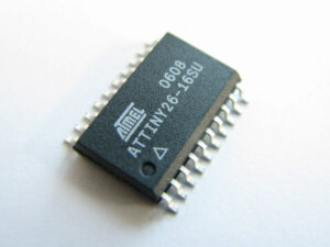
Extract IC ATtiny26 Binary from microcontroller flash memory needs to crack attiny26 microcontroller fuse bit and readout embedded firmware:
Features
- High-performance, Low-power AVR ® 8-bit Microcontroller
- RISC Architecture
– 118 Powerful Instructions – Most Single Clock Cycle Execution
– 32 x 8 General Purpose Working Registers
– Fully Static Operation
– Up to 16 MIPS Throughput at 16 MHz

Data and Non-volatile Program Memory
– 2K Bytes of In-System Programmable Program Memory Flash
Endurance: 10,000 Write/Erase Cycles
– 128 Bytes of In-System Programmable EEPROM
Endurance: 100,000 Write/Erase Cycles
– 128 Bytes Internal SRAM
– Programming Lock for Flash Program and EEPROM Data Security
Peripheral Features
– 8-bit Timer/Counter with Separate Prescaler
– 8-bit High-speed Timer with Separate Prescaler
2 High Frequency PWM Outputs with Separate Output Compare Registers
Non-overlapping Inverted PWM Output Pins
– Universal Serial Interface with Start Condition Detector

– 10-bit ADC
11 Single Ended Channels
8 Differential ADC Channels
7 Differential ADC Channel Pairs with Programmable Gain (1x, 20x)
– On-chip Analog Comparator
– External Interrupt
– Pin Change Interrupt on 11 Pins
– Programmable Watchdog Timer with Separate On-chip Oscillator
Special Microcontroller Features
– Low Power Idle, Noise Reduction, and Power-down Modes
– Power-on Reset and Programmable Brown-out Detection
– External and Internal Interrupt Sources
– In-System Programmable via SPI Port
– Internal Calibrated RC Oscillator
I/O and Packages
– 20-lead PDIP/SOIC: 16 Programmable I/O Lines
– 32-lead MLF: 16 programmable I/O Lines
Operating Voltages
– 2.7V – 5.5V for ATtiny26L
– 4.5V – 5.5V for ATtiny26
Speed Grades
– 0 – 8 MHz for ATtiny26L
– 0 – 16 MHz for ATtiny26
Power Consumption at 1 MHz, 3V and 25°C for ATtiny26L
– Active 16 MHz, 5V and 25°C: Typ 15 mA
– Active 1 MHz, 3V and 25°C: 0.70 mA
– Idle Mode 1 MHz, 3V and 25°C: 0.18 mA
– Power-down Mode: < 1 µA
The ATtiny26(L) is a low-power CMOS 8-bit microcontroller based on the AVR enhanced RISC architecture. By executing powerful instructions in a single clock cycle, the ATtiny26(L) achieves throughputs approaching 1 MIPS per MHz allowing the system designer to optimize power consumption versus processing speed.
The AVR core combines a rich instruction set with 32 general purpose working registers. All the 32 registers are directly connected to the Arithmetic Logic Unit (ALU), allowing two independent registers to be accessed in one single instruction executed in one clock cycle.
The resulting architecture is more code efficient while achieving throughputs up to ten times faster than conventional CISC microcontrollers in the process of extracting ic attiny26 mcu binary file. The ATtiny26(L) has a high precision ADC with up to 11 single ended channels and 8 differential channels. Seven differential channels have an optional gain of 20x after extract IC.
Four out of the seven differential channels, which have the optional gain, can be used at the same time. The ATtiny26(L) also has a high frequency 8-bit PWM module with two independent outputs. Two of the PWM outputs have inverted non-overlapping output pins ideal for synchronous rectification.
The Universal Serial Interface of the ATtiny26(L) allows efficient software implementation of TWI (Two-wire Serial Interface) or SM-bus interface. These features allow for highly integrated battery charger and lighting ballast applications, low-end thermostats, and firedetectors, among other applications.

