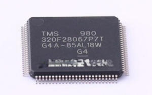
Copying DSP TMS320F28063 Microprocessor Flash Memory Data after clone embedded heximal file to fresh new mcu tm320f28063 and tamper resistance system of microcontroller tms320f28063 will be broken;

Each external interrupt can be enabled/disabled or qualified using positive, negative, or both positive and negative edge. For more information, see the TMS320x280x, 2801x, 2804x DSP System Control and Interrupts Reference Guide (literature number SPRU712).
This section describes the 280x oscillator, PLL and clocking mechanisms, the watchdog function and the low power modes. below Figure shows the various clock and reset domains in the 280x devices which are sharing the same functional blocks of readout dsp microcontroller tms320f28075 flash memory embedded firmware that will be discussed.
The wake-up signal fed to a GPIO pin to wake up the device must meet the minimum pulse width requirement. Furthermore, this signal must be free of glitches. If a noisy signal is fed to a GPIO pin, the wake-up behavior of the device will not be deterministic and the device may not exit low-power mode for subsequent wake-up pulses.

Once the oscillator has stabilized, the PLL lock sequence is initiated, which takes 1 ms.
When CLKIN to the core is enabled, the device will respond to the interrupt (if enabled), after a latency. The HALT mode is now exited when readout tms320f28034 mcu flash data.
Normal operation resumes.
From the time the IDLE instruction is executed to place the device into low-power mode (LPM), wakeup should not be initiated until at least four OSCCLK cycles have elapsed.

