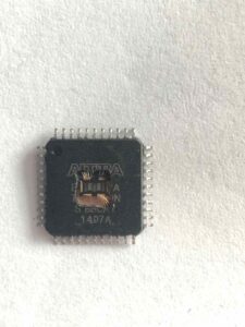
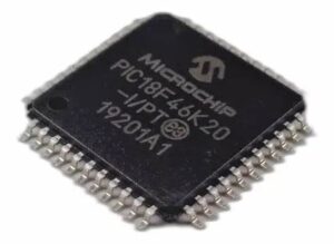
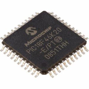
Microchip MCU PIC18F46K20 Source Code Extraction starts from crack microcontroller pic18f46k20 flash memory, the status of mcu memory will reset and make the pic18f46k20 flash program replication become feasible;

The minimum erase block is 32 words or 64 bytes. Only through the use of an external programmer, or through ICSP™ control, can larger blocks of program memory be bulk erased. Word erase in the Flash array is not supported.
When initiating an erase sequence from the Microcon- troller itself, a block of 64 bytes of program memory is erased. The Most Significant 16 bits of the TBLPTR<21:6> point to the block being erased. The TBLPTR<5:0> bits are ignored.

The EECON1 register commands the erase operation. The EEPGD bit must be set to point to the Flash pro- gram memory. The WREN bit must be set to enable write operations. The FREE bit is set to select an erase operation.
The write initiate sequence for EECON2, shown as steps 4 through 6 in Section 6.4.1 “Flash Program Memory Erase Sequence”, is used to guard against accidental writes. This is sometimes referred to as a long write.

A long write is necessary for erasing the internal Flash. Instruction execution is halted during the long write cycle which can be applied as a faulty injection with similar technique of replicating pic18f43k20 mcu secured flash program. The long write is terminated by the internal programming timer.

