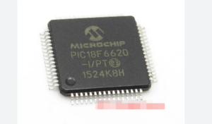
Extract Microchip PIC18F6620 embedded memory content needs to decrypt locked microcontroller PIC18F6620 flash memory program and eeprom memory data, and copy protective microprocessor PIC18F6620 binary file or heximal source code;
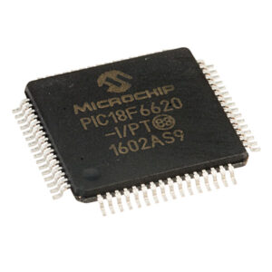
The TRISA register controls the direction of the PORTA pins, even when they are being used as analog inputs. The user must ensure the bits in the TRISA register are maintained set when using them as analog inputs to Extract Microchip PIC18F6620 Embedded Memory. PORTB is an 8-bit wide, bidirectional port.
The corresponding data direction register is TRISB. Setting a TRISB bit (= 1) will make the corresponding PORTB pin an input (i.e., put the corresponding output driver in a high-impedance mode). Clearing a TRISB bit (= 0) will make the corresponding PORTB pin an output (i.e., put the contents of the output latch on the selected pin). The Data Latch register (LATB) is also memory mapped.
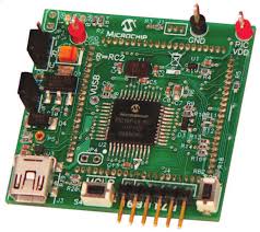
Read-modify-write operations on the LATB register read and write the latched output value for PORTB. Each of the PORTB pins has a weak internal pull-up. A single control bit can turn on all the pull-ups. This is performed by clearing bit, RBPU (INTCON2<7>). The weak pull-up is automatically turned off when the port pin is configured as an output. The pull-ups are disabled on a Power-on Reset to proceed with the operation of Extract Microprocessor PIC16F639 Program.
On a Power-on Reset, PORTB is configured as digital inputs except for RB2 and RB3. RB2 and RB3 are configured as analog inputs when the T1OSCMX bit of Configuration Register 3H is cleared. Otherwise, RB2 and RB3 are also configured as digital inputs.
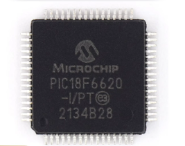
Pins RB0, RB1 and RB4:RB7 are multiplexed with the power control PWM outputs. Pins RB2 and RB3 are multiplexed with external interrupt inputs, interrupt-on-change input, the analog comparator inputs and the Timer1 oscillator input and output to become RB2/INT2/KBI2/CMP2/T1OSO/T1CKI and RB3/INT3/KNBI3/CMP1/T1OSI respectively to facilitate the process of MCU PIC16F636 Flash reading.
