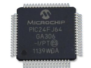
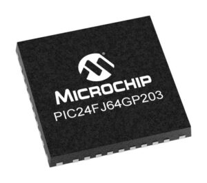
Extract Microchip PIC24FJ64GP203 MCU Source Code from its flash memory and eeprom memory, the protection fuse bit of pic24fj64gp203 microcontroller can be broken, flash memory content inside pic24fj64gp203 microprocessor can be unlock;

Peripheral Pin Select: The Peripheral Pin Select (PPS) feature allows most digital peripherals to be mapped over a fixed set of digital I/O Users may independently map the input and/or output of any one of the many digital peripherals to any one of the I/O pins.
Configurable Logic Cell: The Configurable Logic Cell (CLC) module allows the user to specify combinations of signals as inputs to a logic function and to use the logic output to control other peripherals or I/O when cracking microchip pic24fj64gp202 controller memory file;

Timing Modules: The PIC24FJ64GP205/GU205 family provides three independent, general purpose, 16-bit timers (two of which can be combined into two 32-bit timers). The devices also include five multiple output advanced Capture/Compare/PWM/Timer

Communications: The PIC24FJ64GP205/GU205 family incorporates a range of serial communication peripherals to handle a range of application requirements when copying microchip pic24fj32gp205 controller flash data. There are two independent I2C modules that support both Host and Client modes of Devices also have, through the PPS feature, two independent UARTs with built-in IrDA® encoders/decoders and two SPI modules.
Analog Features: All members of the PIC24FJ64GP205/GU205 family include a 12-bit A/D Converter (ADC) module and a triple comparator module. The A/D module incorporates a range of new features that allow the converter to assess and make decisions on incoming data, reducing CPU overhead for routine A/D conversions. The comparator module includes three analog comparators that are configurable for a wide range of operations.

